1
Date:6/8/2004
SPX3819 500mA, Low Noise LDO Voltage Regulator
© Copyright 2004 Sipex Corporation
500mA, Low-Noise LDO Voltage Regulator
DESCRIPTION
FEATURES
Low Noise: 40µV Possible
High Accuracy: 1%
Reverse Battery Protection
Low Dropout: 340mV at Full Load
Low Quiescent Current: 90µA
Zero Off-Mode Current
Fixed Output: 1.2V, 1.5V, 1.8V, 2.5V, 3.0V,
3.1V, 3.3V, 5.0V
5 Pin SOT-23, 8 Pin nSOIC and 8 pin 2X3 DFN
Packages.
Æ
The SPX3819 is a positive voltage regulator with a low dropout voltage and low noise output. In addition,
this device offers a very low ground current of 800µA at 100mA output. The SPX3819 has an initial tolerance
of less than 1% max and a logic compatible ON/OFF switched input. When disabled power consumption
drop to nearly zero. Other key features include reverse battery protection, current limit, and thermal
shutdown. The SPX3819 includes a reference bypass pin for optimal low noise output performance. With
its very low output temperature coefficient, this device also makes a superior low power voltage reference.
The SPX3819 is an excellent choice for use in battery-powered applications such as cordless telephones,
radio control systems, and portable computers. It is available in several fixed voltages 1.2V, 1.5V, 1.8V,
2.5V, 3.0V, 3.1V, 3.3V, 5.0V or with an adjustable output. This device is offered in 8 pin nSOIC, 8 pin DFN
and 5-pin SOT-23 packages.
APPLICATIONS
Battery Powered Systems
Cordless Phones
Radio Control Systems
Portable/Palm Top/Notebook Computers
Portable Consumer Equipment
Portable Instrumentation
Bar Code Scanners
SMPS Post Regulators
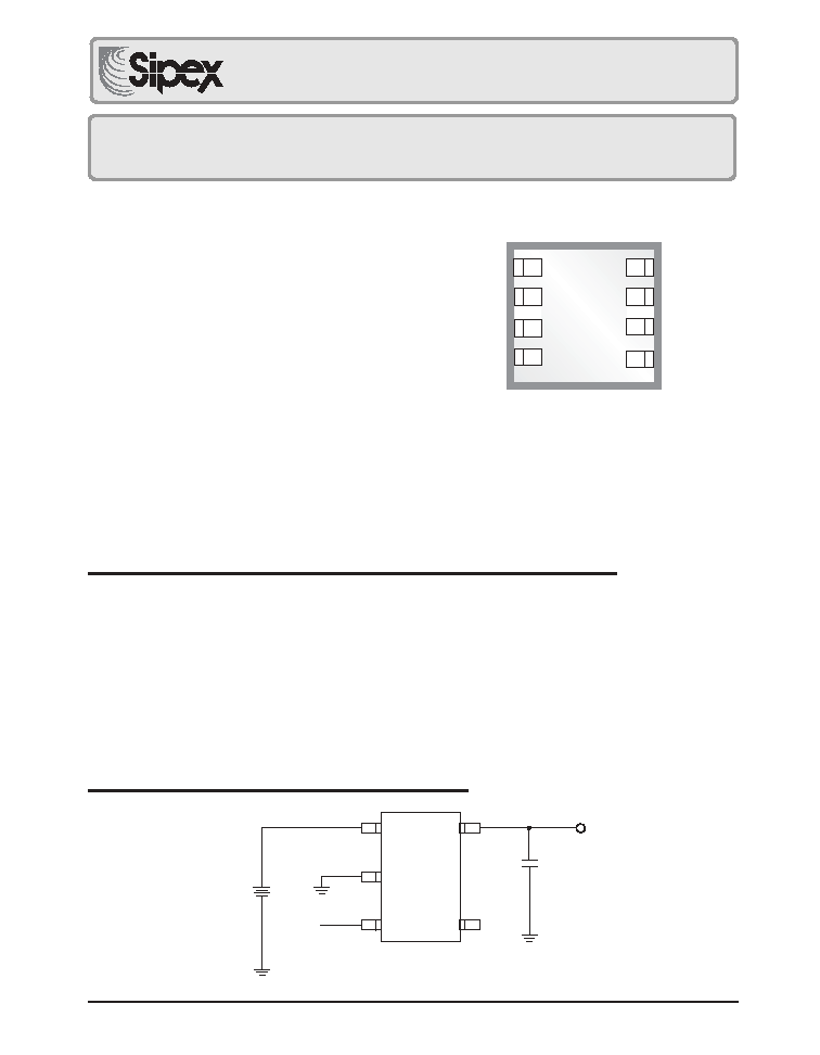
TYPICAL APPLICATION CIRCUIT
+
+
GND
EN
BYP
(Opt.)
ENABLE may be tied directly to V
IN
SPX3819
1
2
3
4
5
V
IN
V
OUT
TOP View
SPX3819
SPX3819
8 Pin DFN
EN
NC
NC
NC
V
IN
ADJ/BYP
V
OUT
GND
5
6
7
8
1
2
3
4
Now Available in Lead Free Packaging
2
Date:6/8/2004
SPX3819 500mA, Low Noise LDO Voltage Regulator
© Copyright 2004 Sipex Corporation
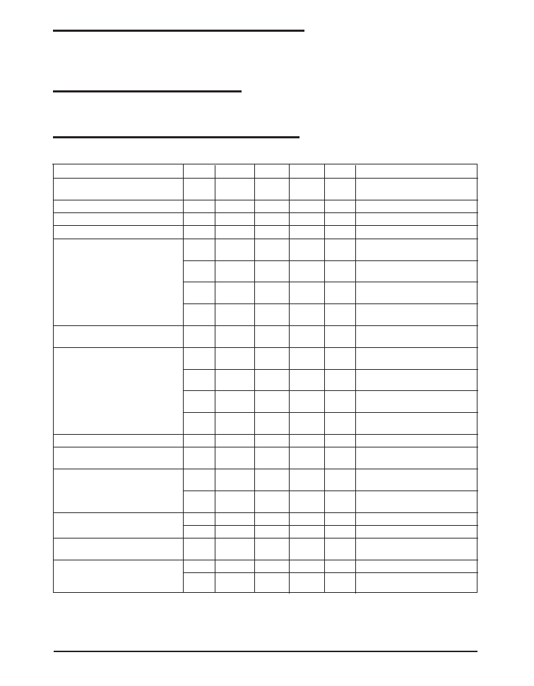
Power Dissipation ...................................................... Internally Limited
Lead Temp. (Soldering, 5 Seconds) ........................................... 260∞C
Operating Junction Temperature Range ................... -40∞C to +125∞C
Input Supply Voltage ........................................................ -20V to +20V
Enable Input Voltage ........................................................ -20V to +20V
PARAMETER
MIN
TYP
MAX
UNITS
CONDITIONS
Output Voltage Tolerance
-1
+1
%
-2
+2
Output Voltage Temperature Coef.
57
ppm/∞C
Line Regulation
0.04
0.1
%/V
V
IN
=V
OUT
+ 1V to 16V
Load Regulation
0.05
0.4
%
I
L
= 0.1mA to 500mA
Dropout Voltage
10
60
mV
I
L
= 100µA
(V
IN
-V
O
)(Note 2)
80
125
175
mV
I
L
= 50mA
250
180
350
mV
I
L
= 150mA
450
340
550
mV
IL = 500mA
700
Quiescent Current (I
GND
)
0.05
3
µA
V
ENABLE
0.4V
8
V
ENABLE
0.25V
Ground Pin Current (I
GND
)
90
150
µA
I
L
= 100µA
190
250
650
µA
I
L
= 50mA
900
1.0
2.0
mA
I
L
= 150mA
2.5
6.5
25.0
mA
I
L
= 500mA
30.0
Ripple Rejection (PSRR)
70
dB
Current Limit (I
LIMIT
)
800
mA
V
OUT
= 0V
950
Output Noise (e
NO
)
300
µV
RMS
I
L
=10mA, C
L
=1.0µF, C
IN
=1µF,
(10Hz-100kHz)
40
µV
RMS
I
L
=10mA, C
L
=10µF, C
BYP
=1µF,
C
IN
=1µF, (10Hz-100kHz)
Input Voltage Level Logic Low (V
IL
)
0.4
V
OFF
Input Voltage Level Logic High (V
IH
)
2
V
ON
ENABLE Input Current
0.01
2
µA
V
IL
0.4V
3
20
V
IH
2.0V
Thermal Resistance (Note 1)
220
∞C/W
SOT-23-5 / Junction to Ambient
180
∞C/W
SO-8 / Junction to Ambient
ELECTRICAL CHARACTERISTICS
T
J
=25
∞C, V
OUT
+ 1V, for 1.2V Option V
IN
=V
OUT
+ 1.2V I
L
=100
µA, C
L
=1
µF, and V
ENABLE
2.4V. The
denotes the
specifications which apply over full operating temperature range -40
∞C to +85∞C, unless otherwise specified.
ABSOLUTE MAXIMUM RATINGS
NOTES
Note 1: The maximum allowable power dissipation is a function of maximum operating junction temperature, T
J(max)
the junction to ambient thermal
resistance, and the ambient
JA
, and the ambient temperature T
A
. The maximum allowable power dissipation at any ambient temperature is
given: P
D(max)
= (T
J(max)
-T
A
)/
JA
, exceeding the maximum allowable power limit will result in excessive die temperature; thus, the regulator will
go into thermal shutdown. The
JA
of the SPX3819 is 220∞C/W mounted on a PC board.
Note 2: Not applicable to output voltage 2V or less.
Input Voltage ................................................................... +2.5V to+16V
Operating Junction Temperature Range ................... -40∞C to +125∞C
Enable Input Voltage .............................................................. 0V to V
IN
RECOMMENDED OPERATIONG CONDITIONS
3
Date:6/8/2004
SPX3819 500mA, Low Noise LDO Voltage Regulator
© Copyright 2004 Sipex Corporation
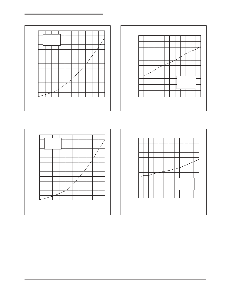
TYPICAL PERFORMANCE CHARACTERISTICS
Ground Current vs Load Current
Ground Current vs Input Voltage
7.0
6.0
5.0
4.0
3.0
2.0
1.0
0.0
0
100
200
300
400
500
I
L
(mA)
I
GND
(mA)
3.3V Device
V
IN
= 4.3V
C
L
= 1.0µF
160
150
140
130
120
110
100
90
80
70
60
4
6
8
10
12
14
16
V
IN
(V)
I
GND
(
µ
A)
3.3V Device
C
L
= 1.0µF
I
L
= 100µA
Ground Current vs Load Current in Dropout
Output Voltage vs Input Voltage
14.0
12.0
10.0
8.0
6.0
4.0
2.0
0.0
0
100
200
300
400
500
I
L
(mA)
I
GND
(mA)
3.3V Device
V
IN
= 4.3V
C
L
= 1.0µF
3.350
3.345
3.340
3.335
3.330
3.325
3.320
3.315
3.310
3.305
3.300
3.295
3.290
4
6
8
10
12
14
16
V
IN
(V)
V
OUT
(V)
3.3V Device
C
L
= 1.0µF
I
L
= 100µA
4
Date:6/8/2004
SPX3819 500mA, Low Noise LDO Voltage Regulator
© Copyright 2004 Sipex Corporation
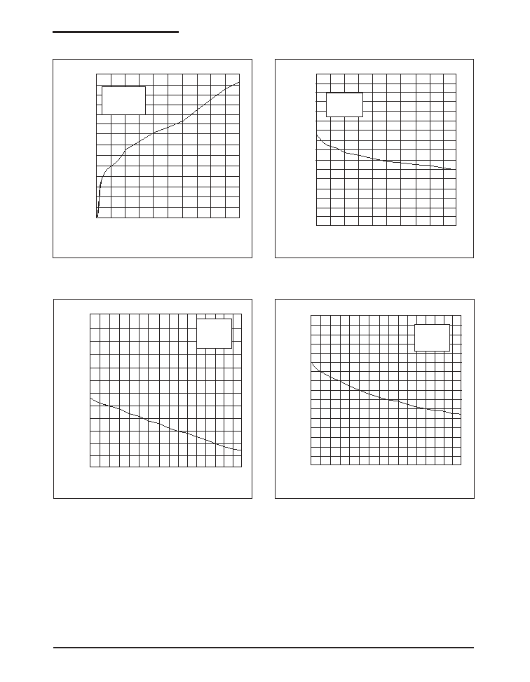
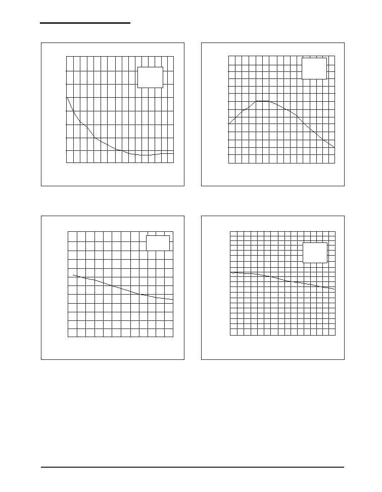
Dropout Voltage vs Load Current
Output Voltage vs Load Current
Ground Current vs Temperature with 100
µA Load
Ground Current vs Temperature with 50mA Load
350
300
250
200
150
100
50
0
0
100
200
300
400
500
I
L
(mA)
Dropout (mV)
3.3V Device
V
IN
= 3.2V
C
L
= 1.0µF
3.316
3.314
3.312
3.310
3.308
3.306
3.304
3.302
3.300
0
100
200
300
400
500
I
L
(mA)
V
OUT
(V)
3.3V Device
V
IN
= 4.3V
C
L
= 1.0µF
130
120
110
100
90
80
70
-40
-20
0
20
40
60
80
100
120
Temperature (∞C)
I
GND
(
µ
A)
3.3V Device
V
IN
= 4.3µF
C
L
= 1.0µF
I
L
= 100µA
360
340
320
300
280
260
240
220
200
-40
-20
0
20
40
60
80
100
120
Temperature (∞C)
I
GND
(
µ
A)
3.3V Device
V
IN
= 4.3
C
L
= 1.0µF
I
L
= 50mA
TYPICAL PERFORMANCE CHARACTERISTICS: Continued
5
Date:6/8/2004
SPX3819 500mA, Low Noise LDO Voltage Regulator
© Copyright 2004 Sipex Corporation
Ground Current vs Temperature with 500mA Load
Ground Current vs Temperature in Dropout
ENABLE Voltage, ON threshold, vs Input Voltage
Output Voltage vs Temperature
8.0
7.5
7.0
6.5
6.0
-40
-20
0
20
40
60
80
100
120
Temperature (∞C)
I
GND
(mA)
3.3V Device
V
IN
= 4.3µF
C
L
= 1.0µF
I
L
= 500mA
14.0
13.5
13.0
12.5
12.0
11.5
11.0
10.5
-40
-20
0
20
40
60
80
100
120
Temperature (∞C)
I
GND
(mA)
3.3V Device
V
IN
= 4.3µF
C
L
= 1.0µF
I
L
= 500mA
1.30
1.25
1.20
1.15
1.10
1.05
1.00
4
6
8
10
12
14
16
V
IN
(V)
V
EN,
On Threshold
(V)
3.3V Device
C
L
= 1.0µF
I
L
= 100µA
3.400
3.380
3.360
3.340
3.320
3.300
2.280
2.260
2.240
2.220
2.200
-40
-20
0
20
40
60
80
100
120
Temperature (∞C)
V
OUT
(V)
3.3V Device
V
IN
= 4.3µF
C
L
= 1.0µF
I
L
= 500mA
TYPICAL PERFORMANCE CHARACTERISTICS: Continued